

2010 Hagen Symposium Reports: Nanostructured PM Materials
A fascinating insight into the world of nanostructured PM materials was given by Prof Bernd Kieback of the Technical University Dresden, Germany, in his Skaupy Presentation at the Hagen Symposium on November 25, 2010 (Fig. 1).
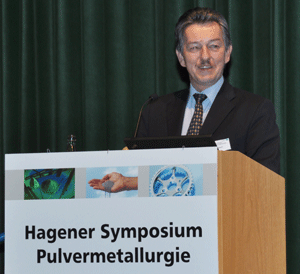
Fig. 1 Prof Bernd Kieback during his Skaupy
speech (courtesy Fachverband Pulvermetallurgie)
Prof Kieback began with a definition of the term ‘nanostructured material’ as being a material with the main phase dimensions significantly below 100 nm. Where this is the case, the volume of phase boundaries relative to the entire volume increases and the bulk properties are affected or even dominated by these disordered areas. The variety of options for the development of nanostructured materials are outlined in Fig. 2.
Many atomic or molecular structures in well-known metals, such as precipitations, have always been nanostructured, however the main constituents, the grains, are much larger. High processing temperatures lead to grain growth which reduces the volume of phase boundaries. Powder metallurgy, as a technology that essentially operates in the solid state, has attractive potentials for the creation of desirable nanostructures.
b) double phase alloy or composite
c) three phases in the nanometer size range
d) nano dispersion strengthened material
e) nano composites with layers between phases
f) nano composites with matrix phase
Fig. 2 Types of nanostructured metals (courtesy B. Kieback)
The PM route to nanostructured materials can either build a material up from nanosized powder or consolidate coarser powders where the nanocrystalline structure has been introduced by the powder production process.
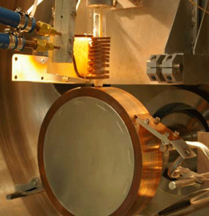
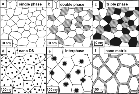
Fig. 3 Melt spinning unit (courtesy B. Kieback)
Working with nanosized powders has the severe disadvantage that large free surface areas are associated with an extremely high reactivity and the tendency of these powders to agglomerate makes it difficult to obtain homogeneous structures. Therefore the second approach is generally preferred. For the preparation of suspensions with functional nanoparticles, however, nanosized powders offer many chances.
Powders in the micrometer size range with nanostructures inside each particle can be produced by several processes. Examples are rapid solidification of a melt (Fig. 3) and mechanical alloying (Fig. 4).
Atomizing processes and melt spinning are capable of cooling rates up to 106 K/s. Certain alloys form amorphous or nanocrystalline structures at this cooling rate. Rapid solidification processes are limited to alloys with solubility in the liquid state.
Fig. 4 Attritor mill used for mechanical alloying
(courtesy B. Kieback)
More flexible in terms of alloy composition are intensive milling processes such as high energy ball milling or attritor milling. These processes, which are also known as mechanical alloying, can combine virtually any constituents independent of solubility limits in the solid or liquid state. Here, too, it is not the target to produce ultra fine powders, but the powder particles are intensively deformed and cold welded again and again. The resulting product is characterised by an extremely high concentrations of lattice defects and dislocations. Many metals develop crystal structures in the range of 10-20 nm even after short milling times.
The intermediate product, powder or strip, is consolidated under pressure at moderate temperatures. Pressureless sintering, the common PM process, is not applicable to nanostructured materials because it would destroy the nanostructures. Hot pressing and extrusion allow reduction of the processing temperature to an extent that the nanostructure of the powder is preserved. Innovative technologies like spark plasma sintering (Fig. 5) are of special interest here because they offer short processing times.
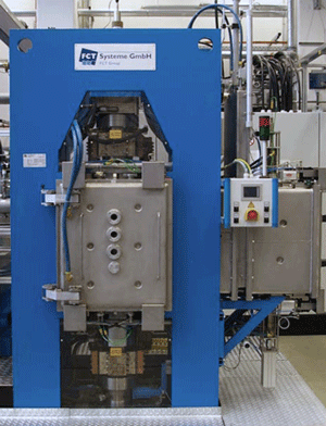
Fig. 5 Spark plasma sintering unit (couresy B. Kieback)
Nanostructured materials find industrial applications where their unique properties lead to cost savings in the entire system or for innovations where no other material solution exists. In comparison with alternative routes, the PM process still offers cost savings. It also has the advantage that up-scaling is possible, both in the product size and in terms of production volume.
An important class in the wide variety of nanostructured materials are dispersion strengthened materials. Finely dispersed nano particles increase the strength and creep resistance of these materials by blocking the sliding of dislocations. The particles should be insoluble in the matrix for long time stability at elevated temperatures. An example is copper dispersion strengthened with TiC. It is made by ball milling a Cu-1.4% Ti prealloyed powder with 0.35% graphite. In a subsequent heat treatment Ti and C combine to form titanium carbide which is insoluble in copper (Fig. 6). The finely dispersed particles lead to an excellent high temperature strength.
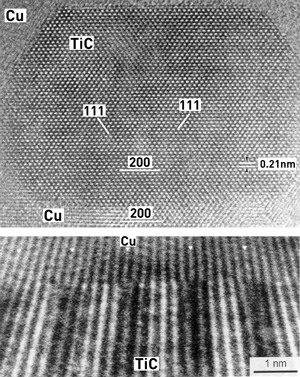
Top: nano TiC particle in Cu matix
Bottom: semi-coherent interface
Fig. 6 Cu-TiC dispersion (courtesy B. Kieback)
Prof Kieback gave many more examples of nanostructured materials. He concluded by saying that there is no universal way to obtain nanostructured PM materials. Depending on the phases present in the material, solid state reactions, grain growth, stability and properties of the individual phases must be considered and controlled in the production process. Due to the many variables involved, computer simulation will certainly be a valuable tool in the future development of nanostructured materials.
Trends in nano powder production and applications
View our extensive report on nano powders as featured in the 14th Edition IPMD 2010-2011
• View PDF report
• Purchase IPMD directory including report
PM2010 World Congress Proceedings
Nanomaterials also featured in the Powder Metallurgy World Congress technical programme. The PM2010 proceedings can be purchsed via our website.
• View nanomaterial presentations
• Purchase PM2010 proceedings
News | Articles | Market reviews | Search directory | Subscribe to e-newsletter